lunes, 15 de febrero de 2010

Cascode:

The cascode is a two-stage amplifier composed of a transconductance amplifier followed by a current buffer. Compared to a single amplifier stage, this combination may

have one or more of the following advantages: higher input-output isolation, higher input impedance, higher output impedance, higher gain or higher bandwidth. In modern

circuits, the cascode is often constructed from two transistors (BJTs or FETs), with one operating as a common emitter or common source and the other as a common base

or common gate. The cascode improves input-output isolation (or reverse transmission) as there is no direct coupling from the output to input. This eliminates the Miller

effect and thus contributes to a much higher bandwidth.


History
:

The cascode (sometimes verbified to cascoding) is a universal technique for improving analog circuit performance, applicable to both vacuum tubes and transistors. The

word "cascode" is a contraction of the phrase "cascade to cathode". It was first used in an article by F.V. Hunt and R.W. Hickman in 1939, in a discussion for application

in low-voltage stabilizers.[1] They proposed a cascode of two triodes (first one with common cathode, the second one with common grid) as a replacement of a pentode.


Operation
:
 
The major advantage of this circuit arrangement stems from the placement of the upper Field Effect Transistor (FET) as the load of the input (lower) FET's output

terminal (drain). Because at operating frequencies the upper FET's gate is effectively grounded, the upper FET's source voltage (and therefore the input transistor's

drain) is held at nearly constant voltage during operation. In other words, the upper FET exhibits a low input resistance to the lower FET, making the voltage gain of the

lower FET very small, which dramatically reduces the Miller feedback capacitance from the lower FET's drain to gate. This loss of voltage gain is recovered by the upper

FET. Thus, the upper transistor permits the lower FET to operate with minimum negative (Miller) feedback, improving its bandwidth.


The upper FET gate is electrically grounded, so charge and discharge of stray capacitance Cdg between drain and gate is simply through RD and the output load (say Rout),

and the frequency response is affected only for frequencies above the associated RC time constant: τ = Cdg RD//Rout, namely f = 1/(2πτ), a rather high frequency because

Cdg is small. That is, the upper FET gate does not suffer from Miller amplification of Cdg.


If the upper FET stage were operated alone using its source as input node (i.e. common-gate (CG) configuration), it would have good voltage gain and wide bandwidth.

However, its low input impedance would limit its usefulness to very low impedance voltage drivers. Adding the lower FET results in a high input impedance, allowing the

cascode stage to be driven by a high impedance source.


If one were to replace the upper FET with a typical inductive/resistive load, and take the output from the input transistor's drain (i.e. a common-emitter (CE)

configuration), the CE configuration would offer the same input impedance as the cascode, but the cascode configuration would offer a potentially greater gain and much

greater bandwidth.


Stability
:

The cascode arrangement is also very stable. Its output is effectively isolated from the input both electrically and physically. The lower transistor has nearly constant

voltage at both drain and source and thus there is essentially "nothing" to feed back into its gate. The upper transistor has nearly constant voltage at its gate and source.

Thus, the only nodes with significant voltage on them are the input and output, and these are separated by the central connection of nearly constant voltage and by the

physical distance of two transistors. Thus in practice there is little feedback from the output to the input. Metal shielding is both effective and easy to provide between

the two transistors for even greater isolation when required. This would be difficult in one-transistor amplifier circuits, which at high frequencies would require

neutralization.


Biasing
:

As shown, the cascode circuit using two "stacked" FET's imposes some restrictions on the two FET's-namely, the upper FET must be biased so its source voltage is high

enough (the lower FET drain voltage may swing too low, causing it to leave saturation). Insurance of this condition for FET's requires careful selection for the pair, or

special biasing of the upper FET gate, increasing cost.


The cascode circuit can also be built using bipolar transistors, or MOSFETs, or even one FET (or MOSFET) and one BJT. In the latter case, the BJT must be the upper

transistor; otherwise, the (lower) BJT will always saturate (unless extraordinary steps are taken to bias it).


Advantages
:

The cascode arrangement offers high gain, high slew rate, high stability, and high input impedance. The parts count is very low for a two-transistor circuit.


Disadvantages
:

The cascode circuit requires two transistors and requires a relatively high supply voltage. For the two-FET cascode, both transistors must be biased with ample VDS in

operation, imposing a lower limit on the supply voltage.


Dual-gate version
:

A dual-gate MOSFET often functions as a "one-transistor" cascode. Common in the front ends of sensitive VHF receivers, a dual-gate MOSFET is operated as a common-

source amplifier with the primary gate (usually designated "gate 1" by MOSFET manufacturers) connected to the input and the 2nd gate grounded (bypassed). Internally,

there is one channel covered by the two adjacent gates; therefore, the resulting circuit is electrically a cascode composed of two FETs, the common lower-drain-to-upper-

source connection merely being that portion of the single channel that lies physically adjacent to the border between the two gates.


Figure 1: N-channel cascode amplifier with resistive load (neglecting biasing details)


Obtenido de: http://en.wikipedia.org/wiki/Cascode


Wilson current mirror:

A Wilson current mirror or Wilson current source is a circuit configuration designed to provide a constant current source or sink. The circuit is shown in the image. It is

named after George Wilson, an integrated circuit design engineer working for Tektronix. Rumour has it that Wilson came up with this configuration after being challenged

to come up with a useful new circuit that used three active devices.


Circuit Analysis:

Assumptions:

1.All transistors have the same current gain β.

2.Q1 and Q2 are matched, so their collector currents are equal.


Therefore, IC1 = IC2 (= IC) and IB1 = IB2 (= IB) ... (1)


Base current of Q3 is given by,

I_{B3} = \frac{I_{C3}}{\beta} ... (2)

and emitter current by,

 I_{E3} = \left(\frac{\beta + 1}{\beta}\right)I_{C3} ... (3)

From the schematic, it is evident that IE3 = IC2 + IB1 + IB2 ... (4)


substituting for IC2, IB1 and IB2 from (1) in (4),

IE3 = IC + 2.IB ... (5)

so,

I_{E3} = I_C\left(1 + \frac{2}{\beta}\right) ... (6)

substituting for IE3 from (3),

\left(\frac{\beta + 1}{\beta}\right)I_{C3} = I_C\left(1 + \frac{2}{\beta}\right)


rearranging,

 I_C = \left(\frac{\beta + 1}{\beta + 2}\right)I_{C3} ... (7)

Current through R1 is given by,

IR1 = IC1 + IB3 ... (8)

But, IC1 = IC2 = IC

Substituting for IC from (7) in (8) and since  we get,

I_{R1} = \left(\frac{\beta + 1}{\beta + 2}\right)I_{C3} + \frac{I_{C3}}{\beta} ... (9)

Therefore,      I_{R1} = \left(\frac{\beta + 1}{\beta + 2} + \frac{1}{\beta}\right)I_{C3}     ... (10)

And finally,


I_{C3} = \frac{I_{R1}}{1 + \frac{2}{\beta(\beta + 2)}} ... (11)

From the above equation we can see that if  \frac{2}{\beta(\beta + 2)} << 1, I_{C3} \approx I_{R1}

And the output current (assuming the base-emitter voltage of all transistors to be 0.7 V) is calculated as,

I_{C3} \approx I_{R1} = \frac{V_{CC} - 1.4}{R1}

Note that the output current is equal to the input current IR1 which in turn is dependent on VCC and R1. If VCC is not stable, the output current will not be stable. Thus

the circuit does not act as a constant current source.


In order for it to work as a constant current source, R1 must be replaced with a constant current source.


Wilson current source


Advantages over other configurations
:

This circuit has the advantage of virtually eliminating the base current mis-match of the conventional current mirror thereby ensuring that the output current IC3 is almost

equal to the reference or input current IR1. It also has a very high output impedance.


Further improvement:
 
Improved Wilson current mirrorAdding a fourth transistor to the Wilson current mirror improves its linearity at higher current levels. It accomplishes this by equalizing

the collector voltages of Q1 and Q2 at 1 Vbe. This leaves the finite beta and voltage differences of each of Q1 and Q2 as the remaining unbalancing influences in the

mirror.


Improved Wilson current mirror


Obtenido de: http://en.wikipedia.org/wiki/Wilson_current_source


Widlar current source:

Diagram from Widlar's original patentA Widlar current source is a modification of the basic two-transistor current mirror that incorporates an emitter degeneration

resistor for only the output transistor, enabling the current source to generate low currents using only moderate resistor values.


The Widlar circuit may be used with bipolar transistors, MOS transistors, and even vacuum tubes. An example application is the 741 operational amplifier, and Widlar

used the circuit as a part in many designs.


This circuit is named after its inventor, Bob Widlar, and was patented in 1967.


Diagram from Widlar's original patent


Analysis:
 
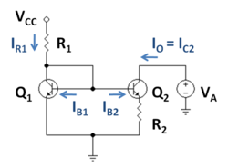
Figure 1: A version of the Widlar current source using bipolar transistors.Figure 1 is an example Widlar current source using bipolar transistors, where the emitter

resistor R2 is connected to the output transistor Q2, and has the effect of reducing the current in Q2 relative to Q1. The key to this circuit is that the voltage drop

across the resistor R2 subtracts from the base-emitter voltage of transistor Q2, thereby turning this transistor off compared to transistor Q1. This observation is

expressed by equating the base voltage expressions found on either side of the circuit in Figure 1 as:


V_B = V_{BE1} = V_{BE2}+(\beta_2+1)I_{B2}R_2 \ ,

where β2 is the beta-value of the output transistor, which is not the same as that of the input transistor, in part because the currents in the two transistors are very

different.[8] The variable IB2 is the base current of the output transistor, VBE refers to base-emitter voltage. This equation implies (using the Shockley diode law):


Eq. 1

(\beta_2+1)I_{B2} =\left(1 + 1/\beta_2 \right) I_{C2} = \frac{V_{BE1} - V_{BE2}}{R_2} = \frac{V_T}{R_2} \ln \left(\frac {I_{C1}I_{S2}}{I_{C2}I_{S1}}\right)\ ,

where VT is the thermal voltage.


This equation makes the approximation that the currents are both much larger than the scale currents IS1, IS2, an approximation valid except for current levels near cut

off. In the following the distinction between the two scale currents is dropped, although the difference can be important, for example, if the two transistors are chosen

with different areas.


Figure 1: A version of the Widlar current source using bipolar transistors.


Output impedance:
 
Figure 2: Small-signal circuit for finding output resistance of the Widlar source shown in Figure 1. A test current Ix is applied at the output, and the output resistance is

then RO = Vx / Ix.An important property of a current source is its small signal incremental output impedance, which should ideally be infinite. The Widlar circuit

introduces local current feedback for transistor Q2. Any increase in the current in Q2 increases the voltage drop across R2, reducing the VBE for Q2, thereby countering

the increase in current. This feedback means the output impedance of the circuit is increased, because the feedback involving R2 forces use of a larger voltage to drive a

given current.


Output resistance is found using a small-signal model for the circuit, shown in Figure 2. The transistor Q1 is replaced by its small-signal emitter resistance rE because it is

diode connected.[10] The transistor Q2 is replaced with its hybrid-pi model. A test current Ix is attached at the output.


Using the figure, the output resistance is determined using Kirchhoff's laws. Using Kirchhoff's voltage law from the ground on the left to the ground connection of R2:


I_b \left( ( R_1 \parallel r_E ) + r_{\pi} \right) + (I_x + I_b ) R_2 = 0 \ .

Rearranging:

I_b = -I_x \frac{R_2}{( R_1 \parallel r_E ) + r_{\pi} +R_2} \ .
Using Kirchhoff's voltage law from the ground connection of R2 to the ground of the test current:


V_x=I_x ( r_O +R_2) +I_b (R_2-\beta r_O)\ ,
or, substituting for Ib:


Eq. 4

R_O = \frac {V_x} {I_x} = r_O \left( 1+ \frac { \beta R_2} {( R_1 \parallel r_E ) + r_{\pi} +R_2} \right)   + \  R_2 \left( \frac { ( R_1 \parallel r_E ) + r_{\pi}} {( R_1 \parallel r_E ) + r_{\pi} + R_2 } \right) \ .

According to Eq. 4, the output resistance of the Widlar current source is increased over that of the output transistor itself (which is rO) so long as R2 is large enough

compared to the rπ of the output transistor. (Large resistances R2 make the factor multiplying rO approach the value (β +1).) The output transistor carries a low current,

making rπ large, and increase in R2 tends to reduce this current further, causing a correlated increase in rπ. Therefore, a goal of R2 >> rπ can be unrealistic, and further

discussion is provided below. The resistance R1//rE usually is small because the emitter resistance rE usually is only a few ohms.


Figure 2: Small-signal circuit for finding output resistance of the Widlar source shown in Figure 1. A test current Ix is applied at the output, and the output resistance is then RO = Vx / Ix


Obtenido de: http://en.wikipedia.org/wiki/Widlar_current_source


Basic MOSFET current mirror:

The basic current mirror can also be implemented using MOSFET transistors, as shown in Figure 2. Transistor M1 is operating in the saturation or active mode, and so is

M2. In this setup, the output current IOUT is directly related to IREF, as discussed next.


The drain current of a MOSFET ID is a function of both the gate-source voltage and the drain-to-gate voltage of the MOSFET given by ID = f (VGS, VDG), a relationship

derived from the functionality of the MOSFET device. In the case of transistor M1 of the mirror, ID = IREF. Reference current IREF is a known current, and can be

provided by a resistor as shown, or by a "threshold-referenced" or "self-biased" current source to ensure that it is constant, independent of voltage supply variations.[1]


Using VDG=0 for transistor M1, the drain current in M1 is ID = f (VGS,VDG=0), so we find: f (VGS, 0) = IREF, implicitly determining the value of VGS. Thus IREF sets

the value of VGS. The circuit in the diagram forces the same VGS to apply to transistor M2. If M2 also is biased with zero VDG and provided transistors M1 and M2 have

good matching of their properties, such as channel length, width, threshold voltage etc., the relationship IOUT = f (VGS,VDG=0 ) applies, thus setting IOUT = IREF; that is,

the output current is the same as the reference current when VDG=0 for the output transistor, and both transistors are matched.


The drain-to-source voltage can be expressed as VDS=VDG +VGS. With this substitution, the Shichman-Hodges model provides an approximate form for function f

(VGS,VDG):[2]


\begin{alignat}{2}   I_{d} & = f\ (V_{GS},V_{DG})         = \begin{matrix} \frac{1}{2}K_{p}\left(\frac{W}{L}\right)\end{matrix}(V_{GS} - V_{th})^2 (1 + \lambda V_{DS}) \\         & =\begin{matrix} \frac{1}{2}K_{p}\left(\frac{W}{L}\right)\end{matrix}(V_{GS} - V_{th})^2 \left( 1 + \lambda (V_{DG}+V_{GS}) \right) \\  \end{alignat}

where, Kp is a technology related constant associated with the transistor, W/L is the width to length ratio of the transistor, VGS is the gate-source voltage, Vth is the

threshold voltage, λ is the channel length modulation constant, and VDS is the drain source voltage.


Figure 2: An n-channel MOSFET current mirror with a resistor to set the reference current IREF; VDD is the supply voltage


Output resistance
:


Because of channel-length modulation, the mirror has a finite output (or Norton) resistance given by the ro of the output transistor, namely (see channel length modulation):


 R_N =r_o = \begin{matrix} \frac {1/\lambda + V_{DS}} {I_D} \end{matrix} ,

where λ = channel-length modulation parameter and VDS = drain-to-source bias.


Compliance voltage
:


To keep the output transistor resistance high, VDG ≥ 0 V [nb 1]. See Baker. [3] That means the lowest output voltage that results in correct mirror behavior, the compliance

voltage, is VOUT = VCV = VGS for the output transistor at the output current level with VDG = 0 V, or using the inverse of the f-function, f −1:


 V_{CV}= V_{GS} (\mathrm{for}\ I_D\ \mathrm{at} \  V_{DG}=0V) = f ^{-1} (I_D) \ \mathrm{with}\  V_{DG}=0  .

For Shichman-Hodges model, f -1 is approximately a square-root function.


Extensions and reservations
:


A useful feature of this mirror is the linear dependence of f upon device width W, a proportionality approximately satisfied even for models more accurate than the

Shichman-Hodges model. Thus, by adjusting the ratio of widths of the two transistors, multiples of the reference current can be generated.


It must be recognized that the Shichman-Hodges model[4] is accurate only for rather dated technology, although it often is used simply for convenience even today. Any

quantitative design based upon new technology uses computer models for the devices that account for the changed current-voltage characteristics. Among the differences

that must be accounted for in an accurate design is the failure of the square law in Vgs for voltage dependence and the very poor modeling of Vds drain voltage dependence

provided by λVds. Another failure of the equations that proves very significant is the inaccurate dependence upon the channel length L. A significant source of

L-dependence stems from λ, as noted by Gray and Meyer, who also note that λ usually must be taken from experimental data.[5]


Feedback assisted current mirror
:

 
Figure 3 shows a mirror using negative feedback to increase output resistance. Because of the op amp, these circuits are sometimes called gain-boosted current mirrors.

Because they have relatively low compliance voltages, they also are called wide-swing current mirrors. A variety of circuits based upon this idea are in use,[6][7][8]

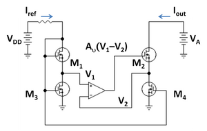
particularly for MOSFET mirrors because MOSFETs have rather low intrinsic output resistance values. A MOSFET version of Figure 3 is shown in Figure 4 where

MOSFETs M3 and M4 operate in Ohmic mode to play the same role as emitter resistors RE in Figure 3, and MOSFETs M1 and M2 operate in active mode in the same roles

as mirror transistors Q1 and Q2 in Figure 3. An explanation follows of how the circuit in Figure 3 works.


The operational amplifier is fed the difference in voltages V1 - V2 at the top of the two emitter-leg resistors of value RE. This difference is amplified by the op amp and

fed to the base of output transistor Q2. If the collector base reverse bias on Q2 is increased by increasing the applied voltage VA, the current in Q2 increases, increasing

V2 and decreasing the difference V1 - V2 entering the op amp. Consequently, the base voltage of Q2 is decreased, and VBE of Q2 decreases, counteracting the increase in

output current.


If the op amp gain Av is large, only a very small difference V1 - V2 is sufficient to generate the needed base voltage VB for Q2, namely


 V_1-V_2 = \frac {V_B}{A_v} \ .


Consequently, the currents in the two leg resistors are held nearly the same, and the output current of the mirror is very nearly the same as the collector current IC1 in Q1,


which in turn is set by the reference current as


 I_{ref} = I_{C1} (1 + 1/ { \beta}_1) \ ,


where β1 for transistor Q1 and β2 for Q2 differ due to the Early effect if the reverse bias across the collector-base of Q2 is non-zero.


Figure 3: Gain-boosted current mirror with op amp feedback to increase output resistance


Figure 4: MOSFET version of wide-swing current mirror; M1 and M2 are in active mode, while M3 and M4 are in Ohmic mode and act like resistors


Output resistance
:

An idealized treatment of output resistance is given in the footnote.[nb 2] A small-signal analysis for an op amp with finite gain Av but otherwise ideal is based upon Figure

5 (β, rO and rπ refer to Q2). To arrive at Figure 5, notice that the positive input of the op amp in Figure 3 is at AC ground, so the voltage input to the op amp is simply

the AC emitter voltage Ve applied to its negative input, resulting in a voltage output of −Av Ve. Using Ohm's law across the input resistance rπ determines the small-signal

base current Ib as:


 I_b = \frac {V_e} {r_{\pi} / ( A_v+1) } \ .


Combining this result with Ohm's law for RE, Ve can be eliminated, to find:[nb 3]


 I_b = I_X \frac {R_E} {R_E +\frac {r_{\pi}} {A_v+1} } \ .

Kirchhoff's voltage law from the test source IX to the ground of RE provides:


 V_X = (I_X + \beta I_b) r_O + (I_X - I_b )R_E \ .


Substituting for Ib and collecting terms the output resistance Rout is found to be:


R_{out} = \frac {V_X} {I_X} = r_O \left( 1+ \beta \frac{R_E} {R_E+r_{\pi}/(A_v+1)} \right) +R_E\|\frac {r_{\pi}} {A_v+1} \ .


For a large gain Av >> rπ / RE the maximum output resistance obtained with this circuit is


R_{out} = ( \beta +1) r_O \ ,


a substantial improvement over the basic mirror where Rout = rO.

The small-signal analysis of the MOSFET circuit of Figure 4 is obtained from the bipolar analysis by setting β = gm rπ in the formula for Rout and then letting rπ → ∞.

The result is
:


R_{out} = r_O \left( 1+ g_m R_E(A_v+1) \right) +R_E \ .

This time, RE is the resistance of the source-leg MOSFETs M3, M4. Unlike Figure 3, however, as Av is increased (holding RE fixed in value), Rout continues to increase,

and does not approach a limiting value at large Av.


Compliance voltage
:

For Figure 3, a large op amp gain achieves the maximum Rout with only a small RE. A low value for RE means V2 also is small, allowing a low compliance voltage for this

mirror, only a voltage V2 larger than the compliance voltage of the simple bipolar mirror. For this reason this type of mirror also is called a wide-swing current mirror,

because it allows the output voltage to swing low compared to other types of mirror that achieve a large Rout only at the expense of large compliance voltages.


With the MOSFET circuit of Figure 4, like the circuit in Figure 3, the larger the op amp gain Av, the smaller RE can be made at a given Rout, and the lower the compliance

voltage of the mirror.


Figure 5: Small-signal circuit to determine output resistance of mirror; transistor Q2 is replaced with its hybrid-pi model; a test current IX at the output generates a voltage VX, and the output resistance is Rout = VX / IX.


Obtenido de: http://en.wikipedia.org/wiki/Current_mirror


Current mirror:

A current mirror is a circuit designed to copy a current through one active device by controlling the current in another active device of a circuit, keeping the output

current constant regardless of loading. The current being 'copied' can be, and sometimes is, a varying signal current. Conceptually, an ideal current mirror is simply an ideal

current amplifier. The current mirror is used to provide bias currents and active loads to circuits.


Mirror characteristics:

There are three main specifications that characterize a current mirror. The first is the current level it produces. The second is its AC output resistance, which determines

how much the output current varies with the voltage applied to the mirror. The third specification is the minimum voltage drop across the mirror necessary to make it work

properly. This minimum voltage is dictated by the need to keep the output transistor of the mirror in active mode. The range of voltages where the mirror works is called

the compliance range and the voltage marking the boundary between good and bad behavior is called the compliance voltage. There are also a number of secondary

performance issues with mirrors, for example, temperature stability.


Practical approximations
:

For small-signal analysis the current mirror can be approximated by its equivalent Norton impedance .

In large-signal hand analysis, a current mirror usually is approximated simply by an ideal current source. However, an ideal current source is unrealistic in several

respects:


  • it has infinite AC impedance, while a practical mirror has finite impedance


  • it provides the same current regardless of voltage, that is, there are no compliance range requirements


  • it has no frequency limitations, while a real mirror has limitations due to the parasitic capacitances of the transistors


  • the ideal source has no sensitivity to real-world effects like noise, power-supply voltage variations and component tolerances.


Circuit realizations of current mirrors
:
 
The simplest bipolar current mirror consists of two transistors connected as shown in Figure 1. Transistor Q1 is connected to ground. Its collector-base voltage is zero as

shown. Consequently, the voltage drop across Q1 is VBE, that is, this voltage is set by the diode law and Q1 is said to be diode connected. (See also Ebers-Moll model.) It is

important to have Q1 in the circuit instead of a simple diode, because Q1 sets VBE for the transistor Q2. If Q1 and Q2 are matched, that is, have substantially the same

device properties, and if the mirror output voltage is chosen so the collector-base voltage of Q2 also is zero, then the VBE-value set by Q1 results in an emitter current in

the matched Q2 that is the same as the emitter current in Q1. Because Q1 and Q2 are matched, their β0-values also agree, making the mirror output current the same as the

collector current of Q1. The current delivered by the mirror for arbitrary collector-base reverse bias VCB of the output transistor is given by (see bipolar transistor):


 I_\mathrm{C} = I_\mathrm{S}  \left( e^{\frac{V_\mathrm{BE}}{V_\mathrm{T}}}-1 \right) \left(1 + \begin{matrix} \frac{V_\mathrm{CB}}{V_\mathrm{A}} \end{matrix} \right)  ,

where VT = thermal voltage, IS = reverse saturation current, or scale current; VA = Early voltage. This current is related to the reference current IREF when the output

transistor VCB = 0 V by:


 I_{REF} = I_C \left( 1+ \frac {2} {\beta_0} \right) \ ,
as found using Kirchhoff's current law at the collector node of Q1. The reference current supplies the collector current to Q1 and the base currents to both transistors ―

when both transistors have zero base-collector bias, the two base currents are equal. Parameter β
0 is the transistor β-value for VCB = 0 V.


Figure 1: A current mirror implemented with npn bipolar transistors using a resistor to set the reference current IREF; VCC = supply voltage


Output resistance:

If VCB is greater than zero in output transistor Q2, the collector current in Q2 will be somewhat larger than for Q1 due to the Early effect. In other words, the mirror

has a finite output (or Norton) resistance given by the rO of the output transistor, namely (see Early effect):


 R_N =r_O = \begin{matrix} \frac {V_A + V_{CB}} {I_C} \end{matrix} ,

where VA = Early voltage and VCB = collector-to-base bias.


Compliance voltage:

To keep the output transistor active, VCB ≥ 0 V. That means the lowest output voltage that results in correct mirror behavior, the compliance voltage, is VOUT = VCV = VBE

under bias conditions with the output transistor at the output current level IC and with VCB = 0 V or, inverting the I-V relation above:


\  V_{CV}= {V_T} \ \mathrm {ln}  \left(\begin{matrix}\frac {I_C}{I_S}\end{matrix}+1\right) \ ,

where VT = thermal voltage  and IS = reverse saturation current (scale current).

Extensions and complications:

When Q2 has VCB > 0 V, the transistors no longer are matched. In particular, their β-values differ due to the Early effect, with

{\beta}_1 = {\beta}_{0} \ \operatorname{and}   \  {\beta}_2 = {\beta}_{0}\ (1 + \frac{V_{CB}}{V_A})
where VA is the Early voltage and β0 = transistor β for VCB = 0 V. Besides the difference due to the Early effect, the transistor β-values will differ because the β0-values

depend on current, and the two transistors now carry different currents (see Gummel-Poon model).

Further, Q2 may get substantially hotter than Q1 due to the associated higher power dissipation. To maintain matching, the temperature of the transistors must be nearly

the same. In integrated circuits and transistor arrays where both transistors are on the same die, this is easy to achieve. But if the two transistors are widely separated,

the precision of the current mirror is compromised.

Additional matched transistors can be connected to the same base and will supply the same collector current. In other words, the right half of the circuit can be duplicated

several times with various resistor values replacing R2 on each. Note, however, that each additional right-half transistor "steals" a bit of collector current from Q1 due to

the non-zero base currents of the right-half transistors. This will result in a small reduction in the programmed current.

An example of a mirror with emitter degeneration to increase mirror resistance is found in two-port networks.

For the simple mirror shown in the diagram, typical values of β will yield a current match of 1% or better.


Obtenido de: http://en.wikipedia.org/wiki/Current_mirror


Espejo de corriente:

En electrónica, un espejo de corriente es una configuración con la que se pretende obtener una corriente constante, esto es, una fuente de corriente. Esta configuración

consta de dos transistores, idealmente idénticos, y una resistencia o potenciómetro, si se quisiera regular el circuito en el caso que los transistores no fueran idénticos. En la

siguiente figura se muestra el esquema básico de un espejo de corriente.


Figura 1: espejo de corriente


Análisis del circuito: 

La Intensidad que circula en R1 está dada por:


IR1 = IC1 + IB1 + IB2

Donde IC1 es la intensidad del colector de Q1, IB1 es la intensidad de base de Q1, IB2 es la intensidad de base de Q2.

La intensidad de colector de Q1 viene dada por la ecuación:

IC1 = β0IB1

Donde β0 es la ganancia de intensidad de Q1. Si Q1 y Q2 son idealmente idénticos, la β de Q2 será:

donde VA es debida al efecto Early.

Desde que VBE1 = VBE2 y Q1 y Q2 son idénticos, IB1 = IB2. La intensidad de colector de Q2 será entonces dado por:

Si β0 > > 1, entonces:

Se obtiene así una precisión superior a la obtenida con circuitos más complejos, como los Widlar, de Wilson o Cascodo.

El espejo de corriente se usa en los circuitos integrados porque es una forma conveniente de crear fuentes de corriente y cargas activas. La ventaja de utilizar espejos de

corriente es la del incremento en la ganancia de tensión y en el rechazo al modo común (CMRR).


Figura 2: espejo de corriente implementado con transistores bipolares tipo NPN usando una resistencia para fijar la intensidad de referencia IREF; VCC = Tensión de entrada


 Obtenido de: http://es.wikipedia.org/wiki/Espejo_de_corriente


FAMILIA CMOS:

Existen varias series en la familia CMOS de circuitos integrados digitales. La serie 4000 que fue introducida por RCA y la serie 14000 por Motorola, estas fueron las

primeras series CMOS. La serie 74C que
su característica principal es que es compatible terminal por terminal y función por función con los dispositivos TTL. Esto hace

posibles remplazar algunos circuitos TTL por un diseño equivalente CMOS. La
serie 74HC son los CMOS de alta velocidad, tienen un aumento de 10 veces la velocidad de

conmutación. La serie 74HCT es también de alta velocidad, y también es compatible en lo que respecta a los voltajes
con los dispositivos TTL.


Los voltajes de alimentación en la familia CMOS tiene un rango muy amplio, estos valores van de 3 a 15 V para los 4000 y los 74C. De 2 a 6 V para los 74HC y 74HCT.


Los requerimientos de voltaje en la entrada para los dos estados lógicos se expresa como un porcentaje del voltaje de alimentación. Tenemos entonces:


VOL(max) = 0 V

VOH(min) = VDD

VIL(max) = 30%VDD

VIH(min) = 70% VDD


Por lo tanto los margenes de ruido se pueden determinar a partir de la tabla anterior y tenemos que es de 1.5 V. Esto es mucho mejor que los TTL ya que los CMOS pueden

ser utlizados en medios con mucho
más ruido. Los margenes de ruido pueden hacerse todavía mejores si aumentamos el valor de VDD ya que es un porcentaje de este.

En lo que a la disipación de potencia concierne tenemos un consumo de potencia de sólo 2.5 nW cuando VDD = 5 V y cuando VDD = 10 V la potencia consumida aumenta a sólo

10 nW. Sin embargo tenemos que
la disipación de potencia sera baja mientras estemos trabajando con corriente directa. La potencia crece en proporción con la frecuencia.

Una compuerta CMOS tiene la misma potencia de disipación en
promedio con un 74LS en frecuencia alrededor de 2 a 3 Mhz.


Ya que los CMOS tienen una resistencia de entrada extremadamente grande (1012 ) que casi no consume corriente. Pero debido a su capacitancia de entrada se limita el

número de entradas CMOS que se
pueden manejar con una sola salida CMOS. Así pues, el factor de carga de CMOS depende del máximo retardo permisible en la

propagación. Comunmente este factor de carga es de 50 para bajas
frecuencias, para altas frecuencias el factor de carga disminuye.

Los valores de velocidad de conmutación dependen del voltaje de alimentación que se emplee, por ejemplo en una 4000 el tiempo de propagación es de 50 ns para VDD = 5 V

y 25ns para VDD = 10 V. Como
podemos ver mientras VDD sea mayor podemos operar en frecuencias más elevadas.


Hay otras características muy importante que tenemos que considerar siempre, las entradas CMOS nunca deben dejarse desconectadas, todas tienen que estar conectadas a

un nivel fijo de voltaje, esto es
por que los CMOS son, al igual que los MOS muy susceptibles a cargas electrostáticas y ruido que podrían dañar los dispositivos.


Características de la familia CMOS:

La tecnología MOS (Metal Oxido Semiconductor) deriva su nombre de la estructura básica MOS de un electrodo metálico montado en un aislador de óxido sobre un subestrato semiconductor. Los

transistores de la tecnología MOS son transistores de campo denominados MOSFET. La mayoría de los CI digitales MOS se construyen exclusivamente con MOSFET.

  • Voltaje de alimentación: Las series 4000 y 74C funcionan con valores de VDD que van de 3 a 15V, por lo que la regulación de voltaje no es un aspecto crítico. Las series
        74HC y 74HCT funcionan con voltajes de 2 a 6 V.


  • Niveles de voltaje: Cuando las salidas CMOS manejan solo entradas CMOS, los niveles de voltaje de la salida pueden estar muy cercanos a 0V para el estado bajo, y a VDD para el estado alto.

VOL (max)
0V
VOH (min)
VDD
VIL (max)
30% VDD
VIH (min)
70% VDD


  • Velocidad de operación: Una compuerta NAND N-MOS común tiene un tiempo de retardo de 50 ns. Esto se debe principalmente a la resistencia de salida relativamente alta (100k) y la carga
        
          capacitiva representada por las entradas de los circuitos lógicos manejados.


  • Margen de ruido: Normalmente, los márgenes de ruido N-MOS están alrededor de 1.5V cuando operan desde VDD = 5 V, y serán proporcionalmente mayores para valores más grandes de VDD.


  •  Factor de carga: Para circuitos operando en DC o de baja frecuencia, las capacidades del factor de carga son virtualmente ilimitadas. Sin embrago, para frecuencias mayores de 100 kHz, se observa

           un deterioro del factor de carga - siendo del orden de 50, lo que es un tanto mejor que en las familias TTL.


  • Consumo de potencia: Los CI MOS consumen pequeñas cantidades de potencia debido a las resistencias relativamente grandes que utilizan. A manera de ejemplo, se muestra la disipación de
        
          potencia del INVERSOR N-MOS en sus dos estados de operación.


          PD = 5V x 0.05nA = 0.25 nW

          PD = 5V x 50 A = 0.25mW


  • Complejidad del proceso: La lógica MOS es la familia lógica más simple de fabricar ya que utiliza un solo elemento básico, el transistor N-MOS (o bien el P-MOS), por lo que no requiere de otros 
        
         elementos como diodos o
resistencias (como el CI TTL).


  • Susceptibilidad a la carga estática:Las familias lógicas MOS son especialmente susceptibles a daños por carga electrostática. Esto es consecuencia directa de la alta impedancia de entrada de estos
         CI. Una pequeña carga electrostática que circule por estas altas impedancias puede dar origen a voltajes peligrosos. La mayoría de los nuevos dispositivos CMOS están protegidos contra daño por

         carga estática mediante la inclusión en sus entradas de un diodo zener de protección. Estos diodos están diseñados para conducir y limitar la magnitud del voltaje de entrada a niveles muy inferiores a los

         necesarios para hacer daño.


Las principales series CMOS son:

·  serie 4000/14000

·  serie 74C

·  serie 74HC (CMOS de alta velocidad)

·  serie 74HCT

·  Diferencias entre las familias TTL y CMOS.


En comparación con las familias lógicas TTL, las familias lógicas MOS son más lentas en cuanto a velocidad de operación; requieren de mucho menos potencia; tienen un mejor manejo del ruido; un mayor

intervalo de suministro de voltaje; un factor de carga más elevado y requieren de mucho menos espacio (área en el CI) debido a lo compacto de los transistores MOSFET. Además, debido a su alta densidad

de integración, los CI MOS están superando a los CI bipolares en el área de integración a gran escala. (LSI - memorias grandes, CI de calculadora, microprocesadores, así como VLSI).

Por otro lado, la velocidad de operación de los CI TTL los hace dominar las categorías SSI o MSI (compuertas, FF y contadores)


Obtenido de: http://html.rincondelvago.com/electronica-digital_9.html