M2. In this setup, the output current IOUT is directly related to IREF, as discussed next.
The drain current of a MOSFET ID is a function of both the gate-source voltage and the drain-to-gate voltage of the MOSFET given by ID = f (VGS, VDG), a relationship
derived from the functionality of the MOSFET device. In the case of transistor M1 of the mirror, ID = IREF. Reference current IREF is a known current, and can be
provided by a resistor as shown, or by a "threshold-referenced" or "self-biased" current source to ensure that it is constant, independent of voltage supply variations.[1]
Using VDG=0 for transistor M1, the drain current in M1 is ID = f (VGS,VDG=0), so we find: f (VGS, 0) = IREF, implicitly determining the value of VGS. Thus IREF sets
the value of VGS. The circuit in the diagram forces the same VGS to apply to transistor M2. If M2 also is biased with zero VDG and provided transistors M1 and M2 have
good matching of their properties, such as channel length, width, threshold voltage etc., the relationship IOUT = f (VGS,VDG=0 ) applies, thus setting IOUT = IREF; that is,
the output current is the same as the reference current when VDG=0 for the output transistor, and both transistors are matched.
The drain-to-source voltage can be expressed as VDS=VDG +VGS. With this substitution, the Shichman-Hodges model provides an approximate form for function f
(VGS,VDG):[2]

where, Kp is a technology related constant associated with the transistor, W/L is the width to length ratio of the transistor, VGS is the gate-source voltage, Vth is the
threshold voltage, λ is the channel length modulation constant, and VDS is the drain source voltage.

Figure 2: An n-channel MOSFET current mirror with a resistor to set the reference current IREF; VDD is the supply voltage
Output resistance:
Because of channel-length modulation, the mirror has a finite output (or Norton) resistance given by the ro of the output transistor, namely (see channel length modulation):
 ,
,where λ = channel-length modulation parameter and VDS = drain-to-source bias.
Compliance voltage:
To keep the output transistor resistance high, VDG ≥ 0 V [nb 1]. See Baker. [3] That means the lowest output voltage that results in correct mirror behavior, the compliance
voltage, is VOUT = VCV = VGS for the output transistor at the output current level with VDG = 0 V, or using the inverse of the f-function, f −1:
 .
.For Shichman-Hodges model, f -1 is approximately a square-root function.
Extensions and reservations:
A useful feature of this mirror is the linear dependence of f upon device width W, a proportionality approximately satisfied even for models more accurate than the
Shichman-Hodges model. Thus, by adjusting the ratio of widths of the two transistors, multiples of the reference current can be generated.
It must be recognized that the Shichman-Hodges model[4] is accurate only for rather dated technology, although it often is used simply for convenience even today. Any
quantitative design based upon new technology uses computer models for the devices that account for the changed current-voltage characteristics. Among the differences
that must be accounted for in an accurate design is the failure of the square law in Vgs for voltage dependence and the very poor modeling of Vds drain voltage dependence
provided by λVds. Another failure of the equations that proves very significant is the inaccurate dependence upon the channel length L. A significant source of
L-dependence stems from λ, as noted by Gray and Meyer, who also note that λ usually must be taken from experimental data.[5]
Feedback assisted current mirror:
Figure 3 shows a mirror using negative feedback to increase output resistance. Because of the op amp, these circuits are sometimes called gain-boosted current mirrors.
Because they have relatively low compliance voltages, they also are called wide-swing current mirrors. A variety of circuits based upon this idea are in use,[6][7][8]
particularly for MOSFET mirrors because MOSFETs have rather low intrinsic output resistance values. A MOSFET version of Figure 3 is shown in Figure 4 where
MOSFETs M3 and M4 operate in Ohmic mode to play the same role as emitter resistors RE in Figure 3, and MOSFETs M1 and M2 operate in active mode in the same roles
as mirror transistors Q1 and Q2 in Figure 3. An explanation follows of how the circuit in Figure 3 works.
The operational amplifier is fed the difference in voltages V1 - V2 at the top of the two emitter-leg resistors of value RE. This difference is amplified by the op amp and
fed to the base of output transistor Q2. If the collector base reverse bias on Q2 is increased by increasing the applied voltage VA, the current in Q2 increases, increasing
V2 and decreasing the difference V1 - V2 entering the op amp. Consequently, the base voltage of Q2 is decreased, and VBE of Q2 decreases, counteracting the increase in
output current.
If the op amp gain Av is large, only a very small difference V1 - V2 is sufficient to generate the needed base voltage VB for Q2, namely
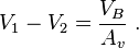
Consequently, the currents in the two leg resistors are held nearly the same, and the output current of the mirror is very nearly the same as the collector current IC1 in Q1,
which in turn is set by the reference current as

where β1 for transistor Q1 and β2 for Q2 differ due to the Early effect if the reverse bias across the collector-base of Q2 is non-zero.

Figure 3: Gain-boosted current mirror with op amp feedback to increase output resistance

Figure 4: MOSFET version of wide-swing current mirror; M1 and M2 are in active mode, while M3 and M4 are in Ohmic mode and act like resistors
Output resistance:
An idealized treatment of output resistance is given in the footnote.[nb 2] A small-signal analysis for an op amp with finite gain Av but otherwise ideal is based upon Figure
5 (β, rO and rπ refer to Q2). To arrive at Figure 5, notice that the positive input of the op amp in Figure 3 is at AC ground, so the voltage input to the op amp is simply
the AC emitter voltage Ve applied to its negative input, resulting in a voltage output of −Av Ve. Using Ohm's law across the input resistance rπ determines the small-signal
base current Ib as:

Combining this result with Ohm's law for RE, Ve can be eliminated, to find:[nb 3]

Kirchhoff's voltage law from the test source IX to the ground of RE provides:

Substituting for Ib and collecting terms the output resistance Rout is found to be:

For a large gain Av >> rπ / RE the maximum output resistance obtained with this circuit is
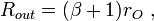
a substantial improvement over the basic mirror where Rout = rO.
The small-signal analysis of the MOSFET circuit of Figure 4 is obtained from the bipolar analysis by setting β = gm rπ in the formula for Rout and then letting rπ → ∞.
The result is:

This time, RE is the resistance of the source-leg MOSFETs M3, M4. Unlike Figure 3, however, as Av is increased (holding RE fixed in value), Rout continues to increase,
and does not approach a limiting value at large Av.
Compliance voltage:
For Figure 3, a large op amp gain achieves the maximum Rout with only a small RE. A low value for RE means V2 also is small, allowing a low compliance voltage for this
mirror, only a voltage V2 larger than the compliance voltage of the simple bipolar mirror. For this reason this type of mirror also is called a wide-swing current mirror,
because it allows the output voltage to swing low compared to other types of mirror that achieve a large Rout only at the expense of large compliance voltages.
With the MOSFET circuit of Figure 4, like the circuit in Figure 3, the larger the op amp gain Av, the smaller RE can be made at a given Rout, and the lower the compliance
voltage of the mirror.

Figure 5: Small-signal circuit to determine output resistance of mirror; transistor Q2 is replaced with its hybrid-pi model; a test current IX at the output generates a voltage VX, and the output resistance is Rout = VX / IX.
Obtenido de: http://en.wikipedia.org/wiki/Current_mirror
No hay comentarios:
Publicar un comentario