domingo, 14 de febrero de 2010

Widlar Current Source

A Widlar current source is a modification of the basic two-transistor current mirror that incorporates an emitter degeneration resistor for only the output transistor, enabling the current source to generate low currents using only moderate resistor values. The Widlar circuit may be used with bipolar transistors, MOS transistors, and even vacuum tubes. An example application is the 741 operational amplifier, and Widlar used the circuit as a part in many designs. This circuit is named after its inventor, Bob Widlar, and was patented in 1967.


File:Widlar Patent.PNG

Analysis


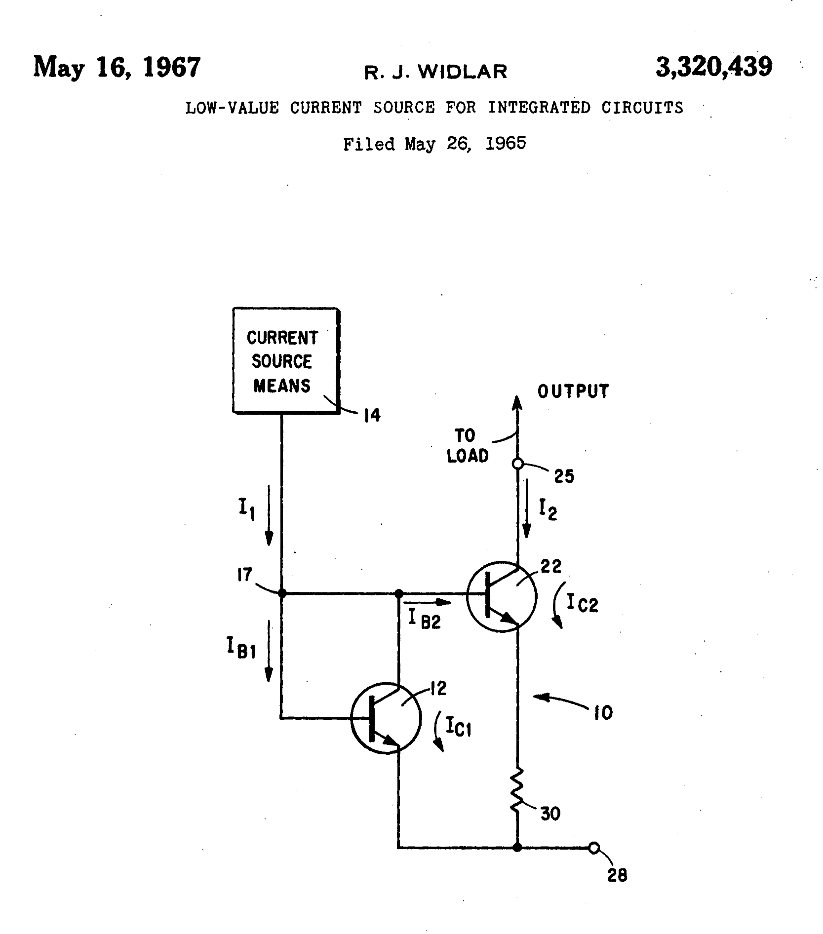
Figure is an example Widlar current source using bipolar transistors, where the emitter resistor R2 is connected to the output transistor Q2, and has the effect of reducing the current in Q2 relative to Q1. The key to this circuit is that the voltage drop across the resistor R2 subtracts from the base-emitter voltage of transistor Q2, thereby turning this transistor off compared to transistor Q1. This observation is expressed by equating the base voltage expressions found on either side of the circuit in Figure as:
V_B = V_{BE1} = V_{BE2}+(\beta_2+1)I_{B2}R_2 \ ,
Where β2 is the beta-value of the output transistor, which is not the same as that of the input transistor, in part because the currents in the two transistors are very different.The variable IB2 is the base current of the output transistor, VBE refers to base-emitter voltage. This equation implies (using the Shockley diode law):

Eq. 1

(\beta_2+1)I_{B2} =\left(1 + 1/\beta_2 \right) I_{C2} = \frac{V_{BE1} - V_{BE2}}{R_2} = \frac{V_T}{R_2} \ln \left(\frac {I_{C1}I_{S2}}{I_{C2}I_{S1}}\right)\ ,
Where VT is the thermal voltage.

This equation makes the approximation that the currents are both much larger than the scale currents IS1, IS2, an approximation valid except for current levels near cut off. In the following the distinction between the two scale currents is dropped, although the difference can be important, for example, if the two transistors are chosen with different areas.


Design Procedure with Specified Currents

To design the mirror, the output current must be related to the two resistor values R1 and R2. A basic observation is that the output transistor is in active mode only so long as its collector-base voltage is non-zero. Thus, the simplest bias condition for design of the mirror sets the applied voltage VA to equal the base voltage VB. This minimum useful value of VA is called the compliance voltage of the current source. With that bias condition, the Early effect plays no role in the design.

These considerations suggest the following design procedure:
  • Select the desired output current, IO = IC2.
  • Select the reference current, IR1, assumed to be larger than the output current, probably considerably larger. (That is the purpose of the circuit.)
  • Determine the input collector current of Q1, IC1:
I_{C1} = \frac{\beta_1}{\beta_1+1} \left( I_{R1}-I_{C2}/\beta_2 \right)\ .
  • Determine the base voltage VBE1 using the Shockley diode law
 V_{BE1} = V_T \ln \left(\frac{I_{C1}} {I_S} \right) = V_A\ .
Where IS is a device parameter sometimes called the scale current.
The value of base voltage also sets the compliance voltage VA = VBE1. This voltage is the lowest voltage for which the mirror works properly.
  • Determine R1:
 R_1 = \frac {V_{CC} - V_A}{I_{R1}}\ .
* Determine the emitter leg resistance R2 using Eq. 1(to reduce clutter, the scale currents are chosen equal):
R_2 = \frac{V_T}{\left(1 + 1/\beta_2 \right) I_{C2}} \ln \left(\frac {I_{C1}}{I_{C2}}\right)\ .
Finding the Current with Given Resistor Values

The inverse of the design problem is finding the current when the resistor values are known. An iterative method is described next. Assume the current source is biased so the collector-base voltage of the output transistor Q2 is zero. The current through R1 is the input or reference current given as,
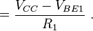
I_{R1} = I_{C1} + I_{B1} + I_{B2} \
= I_{C1} + \frac{I_{C1}}{\beta_1} + \frac{I_{C2}}{\beta_2}
 =  \frac{V_{CC}-V_{BE1}}{R_1} \ .
Rearranging, IC1 is found as:
Eq. 2
I_{C1} =\frac{\beta_1}{\beta_1+1} \left( \frac {V_{CC}-V_{BE1}}{R_1}-\frac{I_{C2}}{\beta_2} \right)
The diode equation provides:
Eq. 3
V_{BE1} = V_T \ln \left( \frac{I_{C1}}{I_{S1}}\right) \ .
Eq.1 provides:
I_{C2}  = \frac{V_T}{\left(1 + 1/\beta_2 \right) R_2} \ln \left(\frac {I_{C1}}{I_{C2}}\right)\ .
These three relations are a nonlinear, implicit determination for the currents that can be solved by iteration.
  • We guess starting values for IC1 and IC2.
  • We find a value for VBE1:
V_{BE1} = V_T \ln \left( \frac{I_{C1}}{I_{S1}}\right) \ .
  • We find a new value for IC1:
I_{C1} =\frac{\beta_1}{\beta_1+1} \left( \frac {V_{CC}-V_{BE1}}{R_1}-\frac{I_{C2}}{\beta_2} \right)
  • We find a new value for IC2:
I_{C2}  = \frac{V_T}{\left(1 + 1/\beta_2 \right) R_2} \ln \left(\frac {I_{C1}}{I_{C2}}\right)\ .
This procedure is repeated to convergence, and is set up conveniently in a spreadsheet. One simply uses a macro to copy the new values into the spreadsheet cells holding the initial values to obtain the solution in short order.

Note that with the circuit as shown, if VCC changes, the output current will change. Hence, to keep the output current constant despite fluctuations in VCC, the circuit should be driven by a constant current source rather than using the resistor R1.

Output Impedance

An important property of a current source is its small signal incremental output impedance, which should ideally be infinite. The Widlar circuit introduces local current feedback for transistor Q2. Any increase in the current in Q2 increases the voltage drop across R2, reducing the VBE for Q2, thereby countering the increase in current. This feedback means the output impedance of the circuit is increased, because the feedback involving R2 forces use of a larger voltage to drive a given current.

Output resistance is found using a small-signal model for the circuit, shown in Figure. The transistor Q1 is replaced by its small-signal emitter resistance rE because it is diode connected. The transistor Q2 is replaced with its hybrid-pi model. A test current Ix is attached at the output.


Using the figure, the output resistance is determined using Kirchhoff's laws. Using Kirchhoff's voltage law from the ground on the left to the ground connection of R2:


I_b \left( ( R_1 \parallel r_E ) + r_{\pi} \right) + (I_x + I_b ) R_2 = 0 \ .
Rearranging:

I_b = -I_x \frac{R_2}{( R_1 \parallel r_E ) + r_{\pi} +R_2} \ .
Using Kirchhoff's voltage law from the ground connection of R2 to the ground of the test current:

V_x=I_x ( r_O +R_2) +I_b (R_2-\beta r_O)\ ,
or, substituting for Ib:
Eq. 4

R_O = \frac {V_x} {I_x} = r_O \left( 1+ \frac { \beta R_2} {( R_1 \parallel r_E ) + r_{\pi} +R_2} \right)   + \  R_2 \left( \frac { ( R_1 \parallel r_E ) + r_{\pi}} {( R_1 \parallel r_E ) + r_{\pi} + R_2 } \right) \ .
According to Eq. 4, the output resistance of the Widlar current source is increased over that of the output transistor itself (which is rO) so long as R2 is large enough compared to the rπ of the output transistor. (Large resistances R2 make the factor multiplying rO approach the value (β +1).) The output transistor carries a low current, making rπ large, and increase in R2 tends to reduce this current further, causing a correlated increase in rπ. Therefore, a goal of R2 >> rπ can be unrealistic, and further discussion is provided below. The resistance R1//rE usually is small because the emitter resistance rE usually is only a few ohms.

Current Dependence of Output Resistance

The current dependence of the resistances rπ and rO is discussed in the article hybrid-pi model. The current dependence of the resistor values is:
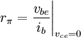

r_{\pi} = \frac{v_{be}}{i_{b}}\Bigg |_{v_{ce}=0}    =\  \frac{V_\mathrm{T}}{I_\mathrm{B2}} = \beta_2\frac{V_\mathrm{T}}{I_\mathrm{C2}}\ , in ohms, and
 r_O = \frac{v_{ce}}{i_{c}}\Bigg |_{v_{be}=0}    =\   \frac {V_A}{I_{C2}}   
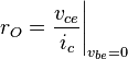
is the output resistance due to the Early effect when VCB = 0 V (device parameter VA is the Early voltage).
From earlier in this article (setting the scale currents equal for convenience):
Eq. 5

R_2 = \frac{V_T}{\left(1 + 1/\beta_2 \right) I_{C2}} \ln \left(\frac {I_{C1}}{I_{C2}}\right)\ .
Consequently, for the usual case of small rE, and neglecting the second term in RO with the expectation that the leading term involving rO is much larger:
Eq. 6

R_O \approx  r_O \left( 1+ \frac { \beta_2 R_2} { r_{\pi} +R_2} \right)  \  =r_O \left( 1+   \frac { \beta_2\ln \left(\frac {I_{C1}}{I_{C2}}\right)} {\left(\beta_2 + 1 \right) + \ln \left(\frac {I_{C1}}{I_{C2}}\right)} \right) \ ,
where the last form is found by substituting Eq. 5 for R2. Eq. 6 shows that a value of output resistance much larger than rO of the output transistor results only for designs with IC1 >> IC2. Figure shows that the circuit output resistance RO is not determined so much by feedback as by the current dependence of the resistance rO of the output transistor. (The output resistance in Figure varies four orders of magnitude, while the feedback factor varies only by one order of magnitude.)

Increase of IC1 to increase the feedback factor also results in increased compliance voltage, not a good thing as that means the current source operates over a more restricted voltage range. So, for example, with a goal for compliance voltage set, placing an upper limit upon IC1, and with a goal for output resistance to be met, the maximum value of output current IC2 is limited.

The center panel in Figure shows the design trade-off between emitter leg resistance and the output current: a lower output current requires a larger leg resistor, and hence a larger area for the design. An upper bound on area therefore sets a lower bound on the output current and an upper bound on the circuit output resistance.

Eq. 6 for RO depends upon selecting a value of R2 according to Eq. 5. That means Eq. 6 is not a circuit behavior formula, but a design value equation. Once R2 is selected for a particular design objective using Eq. 5, thereafter its value is fixed. If circuit operation causes currents, voltages or temperatures to deviate from the designed-for values; then to predict changes in RO caused by such deviations, Eq. 4 should be used, not Eq. 6.


Nombre: Rodriguez B. Joiver I.
Asignatura: EES
 

No hay comentarios:

Publicar un comentario