History
The cascode (sometimes verbified to cascoding) is a universal technique for improving analog circuit performance, applicable to both vacuum tubes and transistors. The word "cascode" is a contraction of the phrase "cascade to cathode". It was first used in an article by F.V. Hunt and R.W. Hickman in 1939, in a discussion for application in low-voltage stabilizers. They proposed a cascode of two triodes (first one with common cathode, the second one with common grid) as a replacement of a pentode.
Operation
Figure shows an example of cascode amplifier with a common source amplifier as input stage driven by signal source Vin. This input stage drives a common gate amplifier as output stage, with output signal Vout.

The major advantage of this circuit arrangement stems from the placement of the upper Field Effect Transistor (FET) as the load of the input (lower) FET's output terminal (drain). Because at operating frequencies the upper FET's gate is effectively grounded, the upper FET's source voltage (and therefore the input transistor's drain) is held at nearly constant voltage during operation. In other words, the upper FET exhibits a low input resistance to the lower FET, making the voltage gain of the lower FET very small, which dramatically reduces the Miller feedback capacitance from the lower FET's drain to gate. This loss of voltage gain is recovered by the upper FET. Thus, the upper transistor permits the lower FET to operate with minimum negative (Miller) feedback, improving its bandwidth.
The upper FET gate is electrically grounded, so charge and discharge of stray capacitance Cdg between drain and gate is simply through RD and the output load (say Rout), and the frequency response is affected only for frequencies above the associated RC time constant: τ = Cdg RD//Rout, namely f = 1/(2πτ), a rather high frequency because Cdg is small. That is, the upper FET gate does not suffer from Miller amplification of Cdg.
If the upper FET stage were operated alone using its source as input node (i.e. common-gate (CG) configuration), it would have good voltage gain and wide bandwidth. However, its low input impedance would limit its usefulness to very low impedance voltage drivers. Adding the lower FET results in a high input impedance, allowing the cascode stage to be driven by a high impedance source.
If one were to replace the upper FET with a typical inductive/resistive load, and take the output from the input transistor's drain (i.e. a common-emitter (CE) configuration), the CE configuration would offer the same input impedance as the cascode, but the cascode configuration would offer a potentially greater gain and much greater bandwidth.
Stability
The cascode arrangement is also very stable. Its output is effectively isolated from the input both electrically and physically. The lower transistor has nearly constant voltage at both drain and source and thus there is essentially "nothing" to feed back into its gate. The upper transistor has nearly constant voltage at its gate and source. Thus, the only nodes with significant voltage on them are the input and output, and these are separated by the central connection of nearly constant voltage and by the physical distance of two transistors. Thus in practice there is little feedback from the output to the input. Metal shielding is both effective and easy to provide between the two transistors for even greater isolation when required. This would be difficult in one-transistor amplifier circuits, which at high frequencies would require neutralization.
Biasing
As shown, the cascode circuit using two "stacked" FET's imposes some restrictions on the two FET's―namely, the upper FET must be biased so its source voltage is high enough (the lower FET drain voltage may swing too low, causing it to leave saturation). Insurance of this condition for FET's requires careful selection for the pair, or special biasing of the upper FET gate, increasing cost. The cascode circuit can also be built using bipolar transistors, or MOSFETs, or even one FET (or MOSFET) and one BJT. In the latter case, the BJT must be the upper transistor; otherwise, the (lower) BJT will always saturate (unless extraordinary steps are taken to bias it).
Advantages
The cascode arrangement offers high gain, high slew rate, high stability, and high input impedance. The parts count is very low for a two-transistor circuit.
Disadvantages
The cascode circuit requires two transistors and requires a relatively high supply voltage. For the two-FET cascode, both transistors must be biased with ample VDS in operation, imposing a lower limit on the supply voltage.
Dual-Gate Version
A dual-gate MOSFET often functions as a "one-transistor" cascode. Common in the front ends of sensitive VHF receivers, a dual-gate MOSFET is operated as a common-source amplifier with the primary gate (usually designated "gate 1" by MOSFET manufacturers) connected to the input and the 2nd gate grounded (bypassed). Internally, there is one channel covered by the two adjacent gates; therefore, the resulting circuit is electrically a cascode composed of two FETs, the common lower-drain-to-upper-source connection merely being that portion of the single channel that lies physically adjacent to the border between the two gates.
Other Applications
With the rise of integrated circuits, transistors have become cheap in terms of silicon die area. In MOSFET technology especially, cascoding can be used in current mirrors to increase the output impedance of the output current source. A modified version of the cascode can also be used as a modulator, particularly for amplitude modulation. The upper device supplies the audio signal, and the lower is the RF amplifier device.
Two-Port Parameters
The cascode configuration can be represented as a simple voltage amplifier (or more accurately as a g-parameter two-port network) by using its input impedance, output impedance, and voltage gain. These parameters are related to the corresponding g-parameters below. Other useful properties not considered here are circuit bandwidth and dynamic range.
BJT Cascode: Low-Frequency Small-Signal Parameters
The idealized small-signal equivalent circuit can be constructed for the circuit in figure by replacing the current sources with open-circuits and the capacitors with short circuits, assuming they are large enough to act as short-circuits at the frequencies of interest. The BJTs can be represented in the small-signal circuit by the hybrid-pi model.

MOSFET Cascode: Low-Frequency Small-Signal Parameters
Similarly the small-signal parameters can be derived for the MOSFET version, also replacing the MOSFET by its hybrid-pi model equivalent. This derivation can be simplified by noting that the MOSFET gate current is zero, so the small-signal model for the BJT becomes that of the MOSFET in the limit of zero base current:
-


 ,
,

The combination of factors gmrO occurs often in the above formulas, inviting further examination. For the bipolar transistor this product is (see hybrid-pi model):
-
 .
.

Low Frequency Design
The g-parameters found in the above formulas can be used to construct a small-signal voltage amplifier with the same gain, input and output resistance as the original cascode (an equivalent circuit). This circuit applies only at frequencies low enough that the transistor parasitic capacitances do not matter. The figure shows the original cascode (top panel) and the equivalent voltage amplifier or g-equivalent two-port (bottom panel). The equivalent circuit allows easier calculations of the behavior of the circuit for different drivers and loads. In the figure a Thévenin equivalent voltage source with Thévenin resistance RS drives the amplifier, and at the output a simple load resistor RL is attached. Using the equivalent circuit, the input voltage to the amplifier is (see article on voltage division):
-
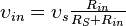 ,
,
In a similar fashion, the output signal from the equivalent circuit is
-
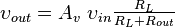 ,
,
The earlier estimate showed that the cascode output resistance is very large. The implication is that many load resistances will not satisfy the condition RL >> Rout. (An important exception is driving a MOSFET as load, which has infinite low frequency input impedance.) However, the failure to satisfy the condition RL >> Rout is not catastrophic because the cascode gain also is very large. If the designer is willing, the large gain can be sacrificed to allow a low load resistance; for RL << Rout the gain simplifies as follows:
-
 .
.
Because the amplifiers are wide bandwidth, the same approach can determine the bandwidth of the circuit when a load capacitor is attached (with or without a load resistor). The assumption needed is that the load capacitance is large enough that it controls the frequency dependence, and bandwidth is not controlled by the neglected parasitic capacitances of the transistors themselves.

High Frequency Design
At high frequencies, the parasitic capacitances of the transistors (gate-to-drain, gate-to-source, drain-to body, and bipolar equivalents) must be included in the hybrid pi models to obtain an accurate frequency response. The design goals also differ from the emphasis on overall high gain as described above for low-frequency design. In high frequency circuits, impedance matching at the input and output of the amplifier is typically desired in order to eliminate signal reflections and maximize power gain. In the cascode, the isolation between the input and output ports still is characterized by a small reverse transmission term g12, making it easier to design matching networks because the amplifier is approximately unilateral.
Nombre: Rodriguez B. Joiver I.
Asignatura: EES
No hay comentarios:
Publicar un comentario